Open student theses
Increasing switching frequencies are placing ever greater demands on signal generation and processing for power electronics applications. Higher switching frequencies allow the use of smaller passive components, but require faster control systems. In order to realize such a control system, a control and actuation system is required that can cope with the increased requirements.
In this work, a microcontroller board based on a state-of-the-art 32-bit, 550MHz processor is used. The aim of the work is to be able to control systems with a minimum time constant of 1µs using the implemented control algorithms.
For this purpose, suitable read-in routines for the system variables, the required control algorithms, the output of the manipulated variable, e.g. via pulse width modulation or discrete-time switching state change, as well as communication interfaces with desktop PCs - for example via UART - are to be created and tested.
The developed system is to be tested in an existing test bench for active load change tests. The various control methods are to be applied and compared in this test bench.
Contact: Tobias Fink
(english version on page 2 of the pdf)
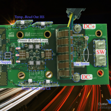
In the evolving electric vehicle market there is a need for highly efficient, power dense and reliable power electronics. In the project frame of KDT Archimedes 1200 V SiC devices used in traction inverters are investigated with respect to reliability. In the frame of the project ultra high operating hours of 120,000 h and more should be verified within a reasonable labor time frame, thereby requiring large acceleration factors without changing the underlying failure mechanisms. While for mature technology of Silicon power devices sophisticated life time models exist such models are only limited applicable for SiC due to the different technology and physics due to higher electric field and current densities.
In this work, degradation sensitive electrical parameters for SiC MOSFETs are to be investigated. For this new measurement circuits based on existing methods are to be developed. The acquisition of data will be performed in power cycling test benches. Based on the stresses induced during the power cycling tests, the State-of-Health of the semiconductor device is to be determined a posteriori based on the in-situ measurements taken.
Helpful previous knowledge:
• RPSS 2
• PE 2/LE 2
• Sensor and measurement technology
• Microcontroller programming (STM32)
Due to ever increasing power densities, number of devices and the use of wide-bandgap semiconductors, power electronic systems are getting more complex and compact. To still achieve a maximum efficiency, all solutions of the (discrete) solution space must be investigated. The solution space is defined by e.g. suitable semiconductors and passives or the PCB-design.
To map this solution space, the aid of computer-based methods is necessary, which are calculating the optimal point of the so called pareto-front.
Goal of this thesis is to implement a workflow for such a pareto-front optimization with a multi-dimensional simulation for a compact DC/DC-converter and, if applicable, to construct and characterize this converter.
Time plan
- Literature research (10%)
- Implementation multi-domain optimization (50%)
- Setup and characterization of the converter (25%)
- Written thesis & talk (20%)
Preliminary experience
- Experience in 3D-FEM helpful
- Knowledge in power electronics
- Good knowledge of MATLAB or similar
Contact

Dominik Koch
M.Sc.Group Leader Power Electronics / Research Assistant

Benjamin Schoch
M.Sc.Research Assistant