Open student theses
Motivation:
Die stetig wachsende Bedarf an immer höheren Datenraten in drahtlosen Kommunikationssystemen erfordert die Erschließung neuer Frequenzbereiche. Die Entwicklung analoger Tx- / Rx-Frontends im THz-Frequenzbereich (~ 220 – 330 GHz) stellt dabei große Herausforderungen an das Schaltungsdesign der einzelnen Komponenten.
Ziele:
- Entwicklung und Evaluierung verschiedener Schaltungstopologien für Mischer, Frequenzmultiplizierer oder Verstärker im THz-Frequenzbereich (~ 220-330 GHz)
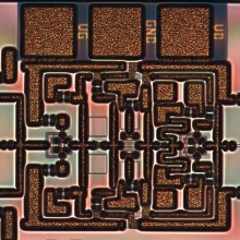
- Circuit Design und Layout der Konzepte in einer III-IV Halbleitertechnologie
Aufgaben:
- Evaluierung vorhandener Entwürfe
- Entwicklung neuer Konzepte
- Circuit-level Simulationen mit ADS
- 3D Feld-Simulationen mit CST/Momentum
- MMIC Layout mit Cadence
- Literaturrecherche
Charakteristisch für eine konventionelle Mikrostreifenleitung ist u. a. eine homogene GND Metallfläche. Um die elektrischen Eigenschaften einer solchen Leitung zu beeinflussen, können in die ebene GND-Fläche bestimmte Muster in der Metalisierung eingeführt werden. Voruntersuchungen haben gezeigt, dass periodische Schlitze in einem bestimmten Abstand die Leitung auf mehreren Weisen positiv beeinflussen.
Goals of this work:
- wissenschaftliche Analyse bestimmter Muster in der GND-Fläche
- Optimierung bestimmter elektrischer Eigenschaften
- Aufsetzen einer full 3D-EM Simulation (Abb. 3)
- Modellierung einer Mikrostreifenleitung für den Entwurf in ADS
Das Einbringen bestimmter Muster in der GND-Fläche stellt dabei in einerIII-V-Technologie eine große Besonderheit dar!
Motivation:
A novel FMCW radar principle operates without an explicit local oscillator signal in the receiver, but relies on self-mixing of the receiver.
Goals:
Developement of circuit parts for a SiGe based Radar Transceiver MMIC.
Tasks:
a.o.:
- Design and simulation of a selected analog circuits e.g. mixer, amplifier, multiplier
- MMIC layout and verification
Please refer to PDF for more details.
Our research group develops analog frontends for THz wireless communication systems operating in H-band (220-325 GHz).
In scope of the SOLITONIC project, it is required to implement an integrated envelope detection functionality in the power amplifier monolithic integrated circuit in order to enable and investigate analog and digital pre-distortion techniques.
The goal of this thesis is to design a monolithic integrated envelope detector circuit operating at a center frequency of 300 GHz.
You will use the state-of-the-art 35 nm InGaAs HEMT technology from the Fraunhofer Institute of Applied Solid-State Physics, which has cutting-edge high frequency and low noise performance and achieves cutoff frequencies (f_max) of well beyond 1 THz.
The task includes the choice of the most appropriate circuit architecture, linear and non-linear circuit analysis, optimization and the creation of a production-ready MMIC layout. A focus is on high circuit compactness for on-chip co-integration of the envelope detector circuit with the PA stage.
The workload will be adjusted according to which kind of thesis you execute.
Our research group develops analog frontends for THz wireless communication systems operating in H-band (220-325 GHz).
In scope of the SOLITONIC project, several active and passive components need to be designed to provide the pre-distortion functionalities of the monolithic integrated power amplifier circuit.
Active:
-Controllable phase shifter and attenuator
-Active power divider
-Buffer amplifier
Passive:
-2- and 3-way power divider
-2- and 3-way power combiner
-Coupler
The goal of this thesis is to design and optionally layout some of these components operating at a center frequency of 300 GHz. For that, circuit simulations and electro-magnetic simulations need to be conducted.
You will use the state-of-the-art 35 nm InGaAs HEMT technology from the Fraunhofer Institute of Applied Solid-State Physics, which has cutting-edge high frequency and low noise performance and achieves cutoff frequencies (f_max) of well beyond 1 THz.
The workload will be adjusted according to which kind of thesis you execute.
Ultra-wideband power amplifier become more and more
important for high-speed data transmission like it is planned in
6G communication networks.
Thereby, a flat gain shape response of a total system is required
for those highspeed data communication systems.
An imbalance in the gain of e.g., a transmitter leads into
different power densities in different channels, which is
unwanted.
Additionally, the fact that the insertion loss of passive
components in the communication system like in cables, or
transmission lines rise with frequency, affects the gain
response of the total system [Fig. 1].
To overcome now this issue a peaking ultra-wideband amplifier
with increasing gain shape over frequency can be
implemented.
The goal of this amplifier is to compensate the rising losses of
those passives in order so lead into an overall flat gain and
power response of the total communication system.
With different kind of peaking techniques, a gain response of a
peaking amplifier as depicted in Fig. 2 can be reached.
Our research group develops analog frontends for THz wireless communication
systems operating in H-band (220-325 GHz).
In scope of the SOLITONIC project,
an analog pre-distortion operating at a center frequency of 300 GHz will be developed. One approach for the realization of the analog pre-distortion is to exploit the complementary properties of expanding and compressing amplifier classes. For compressing amplifier classes (class A/AB) we have valid simulation models for the transistors available. Expanding amplifier classes (class B/C) are not modeled accurately, because these nonlinear expanding amplifiers can not be used independently for communication purposes. In order to get insights, we need measurements of the class
B/C biased amplifiers.
The goal of this thesis is to design and create a production-ready layout of a single-
stage class B/C amplifier operating at a center frequency of 300 GHz. For that, circuit simulations and electro-magnetic
simulations need to be conducted. You will use the state-of-the-art 35 nm InGaAs HEMT technology from the Fraunhofer Institute of Applied Solid-State Physics, which has cutting-edge high frequency and low noise performance and achieves cutoff frequencies (f_max) of well beyond 1 THz
Motivation: For a reliable, robust, long-distance communication, power amplifiers with high output powers are needed in many cases. By their nature, the amplifiers suffer from the nonlinearities at high power levels. In order to avoid the impairments caused by the nonlinearities which degrade the signal quality and the spectral efficiency, analog & digital pre-distortion techniques are widely employed in the literature. Before proceeding the signal to the amplifier, by purposely distorting the signal and manipulating the distorted signal in terms of amplitude and phase afterwards, the inverse of the spectral products generated by the nonlinearities, can be obtained.Thus, the pre-distorted signal can be fed to the amplifier accompanied by the actual signal and the unwanted frequency products can be canceled out or suppressed and the linear range of the amplifier can be enhanced.
Goals: Realize a schematic / layout design of a circuit in a 130 nm SiGe HBT technology in the V-band, which purely generates IM3 products and suppress the fundamental carriers at the output. The IM3 generator should be adaptive against the errors in the large signal transistor models, fabrication tolerances and changes in the input power levels.
Tasks:
- Comprehensive literature research related to the subject.
- Schematic & layout design and verification of the circuit through the simulations.
- Corner-case simulations and stability analysis.
- Scientific report of the work including the state-of-the-art comparison
Motivation: For a reliable, robust, long-distance communication, power amplifiers with high output powers are needed in many cases. By their nature, the amplifiers suffer from the nonlinearities at high power levels. As a result of the nonlinearities, strong unwanted intermodulation products, higher harmonic spurs can be generated and consequently, the spectral purity of the signal can be degraded. In a transmitter (TX) microwave frontend chain, generally, the power amplifier is the key the component determining the overall linearity of the TX chain. Therefore, the power amplifiers are expected to exhibit high linearity along with the high amplification.
Goals: Realize a schematic / layout design of a power amplifier circuit in 130-nm SiGe HBT technology in the Q-Band. The power amplifier should meet the linearity and gain requirements. Furthermore, the layout compactness of the amplifier should be taken into consideration.
Tasks:
- Comprehensive literature research related to the subject.
- Schematic & layout design and verification of the circuit through the S-Parameters & Harmonic Balance simulations.
- Meticulous & detailed stability analysis of the amplifier.
- Scientific report of the work including the state-of-the-art comparison
Contact

Dominik Koch
M.Sc.Group Leader Power Electronics / Research Assistant

Benjamin Schoch
M.Sc.Research Assistant