Wide-Bandgap Semiconductors

Characterization is the first step to properly design power electronic circuits. A good knowledge of the semiconductor devices enables the optimal utilization of the devices capabilities in the application. The work at ILH in the field of characterization is focused on semiconductor devices based on novel wide-bandgap materials such as GaN and SiC. Modeling is an important aspect to predict the behavior of electronic systems in simulations. This enables the optimization of the circuit during its design phase prior to the first prototype building. An accurate simulation requires a detailed model which describes the transistor behavior in all operation regions. Moreover, transistor models must also ease the circuit simulators' convergence and be computational efficient. The ILH concentrates research on development of equivalent circuit based transistor models for SiC and GaN power devices.

Open student theses

In modern power electronics an ever increase in power density and efficiency is pursued. Therefore soft-switching of wide-bandgap semiconductors for high system performance is utilized. While high system advantages can be achieved, the prediction of those soft-switching losses become particular difficult with electrical measurements. Therefore time-consuming calorimetric measurements are utilized to characterize those losses accurately. Only recently time-efficient calorimetric measurement approaches have been developed which simplifies the extraction of the influence of several parameters, but a matching simulative approach is still missing. For a further investigation of several different parameters a hybrid approach of simulating and measurement is pursued. Besides the investigation of different parameters an improved and cost-efficient thermal layout of the soft-switching converters via virtual prototyping can be achieved and an optimization of e.g. the gate driver circuit is feasible.

Timeplan:

  • Familirization & literature research (10%)
  • Simulation of soft-switching losses and simulation model verification (25%)
  • Simulation of different parameters and gate drive circuits (50%)
  • Thesis writing and presentation (15%)

Helpful previous knowledge:

  • Power electronics/ RPSS 1 & RPSS 2
  • Matlab
  • LT-Spice/FEM-Simulations

Kontakt: Ruben Schnitzler

PDF

In modern power electronics an ever increase in power density and efficiency is pursued. Therefore soft-switching of wide-bandgap semiconductors for high system performance is utilized. While high system advantages can be achieved, the prediction of those soft-switching losses become particular difficult with electrical measurements. Therefore time-consuming calorimetric measurements are utilized to characterize those losses accurately. Only recently time-efficient calorimetric measurement approaches have been developed which simplifies the extraction of the influence of several parameters. The output capacitance is the most influencial parameter on the switching losses, but a deep analysis of its dependencies is still missing. Since the output capacitance is dependent on several parameters such as the gate source and source-drain capacitance.

Goal of this work:

  • Implementing a SCPI-programmable DC-source for variable gate source voltage setting
  • Measure the soft-switching losses for different gate source and gate drain voltages.
  • Extract the output capacitanc characteristic

Timeplan:

  • Familirization & Literature research (10%)
  • Implementing DC-Source (30%)
  • Measurement (45%)
  • Thesis writing and presentation (15%)

Helpful Previous knowledge:

  • Power electronics/ RPSS 1 & RPSS 2
  • Matlab
  • Altium/PCB-design

Kontakt: Ruben Schnitzler

PDF

Die Super-junction-Struktur ist einer der vorgeschlagenen Ansätze, um die gewünschte zweidimensionale Ladungskopplung innerhalb von Leistungs-MOSFET-Strukturen zu erreichen. Sie eignet sich gut für die Entwicklung von Si-Leistungs-MOSFET-Strukturen mit großer Sperrspannungsfähigkeit.

Die Bauelementstruktur der modernen Super-junction-Leistungs-MOSFETs unterscheidet sich typischerweise stark von herkömmlichen lateralen MOSFETs. Dies führt dazu, dass die für die lateralen Bauelementmodelle definierten Standardmodelle nicht direkt für Leistungs-MOSFETs mit Super-junction-Strukturen verwendet werden können.

Die Schaltfähigkeiten von Leistungstransistoren werden durch ihre paraitären Kapazitäten und intrinsischen Widerstände bestimmt. Ein präzises Modell für die Kapazität des Transistors ist daher wichtig, um sein Schalterverhalten vorherzusagen. Die meisten Kapazitätsmodelle, die von den Bauelementherstellern zur Verfügung gestellt werden, sind jedoch nicht genau genug.

Die Aufgaben:

  • Untersuchung der Super-junction Struktur und deren Einfluss auf die charakteristischen Eigenschaften des Leistungs-MOSFETs.
  • Untersuchung der Kapazitätsstruktur und der Definition eines Kapazitäten-Modells in einem Leistungs-MOSFET.
  • Beitrag zur Verbesserung und Entwicklung der Kapazitätsmodellierung auf dem Gebiet der Super-Junction-Leistungstransistoren auf der Grundlage des Standardmodells.

PDF

Silicon Carbide is a wide bandgap material and becoming a very attractive choice of semiconductor for high density and high-efficiency power electronics in high voltage range. Power MOSFETs are one of the most commonly used power devices due to their low gate drive power, small device size, fast switching speed, and superior paralleling capability. Therefore, there is an increasing need for accurate and compact models for SiC power MOSFETs which can be used for CAD tools for circuit designers.

The structure of a power SiC MOSFET can be similar to the vertical Si power MOSFETs, but the different properties of the materials and the fabrication technology cause their quite different characteristics.

The aim of this research is to evaluate the requirements of the specific definitions of the SiC power MOSFET model. The standard compact model used in the silicon industry can be adopted as a foundation to build the model for SiC MOSFET.

Tasks:

  • Study therequirementsanddefinitionsofSiCpower transistor models
  • Understand the static and dynamic characteristics of a power MOSFET
  • Understand different modelingapproachesforSiCpower transistors
  • Contribute to the improvement and development of modeling in the field of power transistors based on the standard model.

PDF

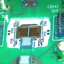
Transistoren auf Basis von Galliumnitrid (GaN) gelten als vielversprechende Bauteile, um fundamentale, materialbedinge Beschränkungen siliciumbasierter Leistungstransistoren zu übertreffen. Doch neben ihren positiven Eigenschaften trüben einige Nachteile das sonst positive Gesamtbild. Eines dieser Probleme ist der sog. „Dynamische RDS,on-Effekt“, welcher die temporäre Erhöhung des Durchgangswiderstandes unmittelbar nach dem Einschalten beschreibt. Gerade bei höheren Schaltfrequenzen, welche durch die Nutzung von GaN-HEMTs angestrebt werden, spielt dieser Effekt also eine große Rolle. In dieser studentischen Arbeit soll der dynamische On-State-Widerstand eines HEMTs vermessen und der Einfluss verschiedener äußerer Parameter untersucht werden.

Arbeitspunkte

  • Einarbeitung in die Thematik des dynamischen RDS,on-Effektes
  • Einarbeitung in die zugrunde liegende Messmethodik
  • Design von Platinen für die Vermessung der HEMTs
  • Durchführung von Messreihen, Analyse der erhobenen Daten
  • Datenauswertung
  • Ausarbeitung und Vortrag

Kontakt: Mathias Weiser

PDF

Bedingt durch ihre vorteilhaften Materialeigenschaften sind Transistoren aus Galliumnitrid (GaN) auch für leistungselektronische Anwendungsbereiche attraktiv. Lange Zeit waren für Transistoren dieser Art allerdings nur empirische Modelle verfügbar. In jüngster Vergangenheit wurden von der „Compact Modelling Coalition“, einer Interessengemeinschaft für die Standardisierung von Simulationsmodellen, zwei physikalisch basierte Modelle als Industriestandard vorgeschlagen: das „MIT Virtual Source GaN“ (MVSG) des MIT, sowie das „Advanced Spice Model for HEMTs“ (ASM-HEMT) des IIT Kanpur. In dieser studentischen Arbeit sollen für einen vorliegenden Transistor für beide Modelle ein Parametersatz extrahiert und beide Modelle hinsichtlich ihrer Eigenschaften verglichen werden.

Arbeitspunkte

  • Einarbeitung in die Funktionsweise von MVSG und ASM-HEMT
  • Charakterisierung eines GaN-HEMTs mit einem Semiconductor Device Analyser
  • Parameterextraktion
  • Prüfung der resultierenden Transistormodelle
  • Ausarbeitung und Vortrag

Kontakt: Mathias Weiser

PDF

This image shows Benjamin Schoch

Benjamin Schoch

M.Sc.

Research Assistant

To the top of the page