This project addresses the research area “Advanced design methodologies for testing next generation and beyond RF devices” by proposing a miniaturized and multi-functional frequency extension into the high millimeter-wave frequency range for RF testing.
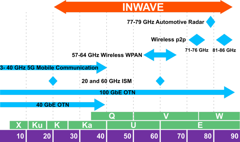
One goal of this project is to cover the frequency range from 20 to 86 GHz to enable testing for applications such as 24 GHz ISM i.e. from K-band to E-band, including important frequency ranges like 77-79 GHz for automotive radar or 81-86 GHz fixed wireless point-to-point links by using high-speed semiconductor technologies (see Figure 1).
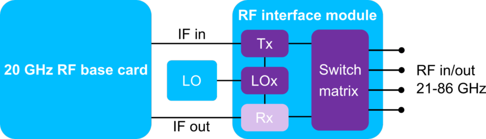
The transceiver module is designed to be coupled to a 20 GHz RF base card from Advantest.
The project covers the most challenging components of an entire transceiver chain including RF up-conversion, RF multi-pole switching, RF adaptive power amplification, RF filtering and LO multiplication over the entire frequency range (see Figure 2).
In order to meet the challenging requirements of wide frequency range, high linearity and high output power and at the same time achieve a high level of system integration, it will probably become necessary to design and combine different parts of the system in different semiconductor technologies, e.g., RF-CMOS, GaN, InP or GaAs.
Therefore, this project is divided into two main phases. In the first project phase a deep investigation of all commercially available technologies will be made. After that a line-up will be created to allow a detailed simulation of each sub-block. Two approaches will be considered: a hybrid version that will select the most suitable semiconductor technology for each element of the design, and a compact system-on-chip (SoC) version based on a state-of-the-art CMOS process (e.g., 22nm FD-SOI).
After this first phase a decision about the target technology will be made together with Advantest to initiate the second phase of this project.
At the beginning of this phase the circuit design and layout with a full-3D simulation of the whole system will be performed. In order to optimize the design, three fabrication cycles are planned.
Depending on the chosen packaging technology the assembly will also be designed.
Finally the project ends with the testing and measurement of the developed system.

Athanasios Gatzastras
M.Sc.Research Assistant